



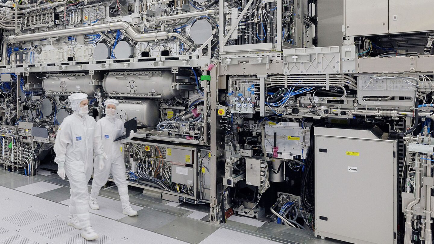
Samsung and TSMC are set to join Intel in adopting ASML’s latest High Numerical Aperture (High NA) extreme ultraviolet (EUV) lithography technology, in a move aimed at improving the production of increasingly advanced semiconductors. ASML announced the commitments as the chip industry continues to invest in manufacturing technologies that can produce smaller, more complex components.
Samsung plans to introduce the technology for DRAM memory production by 2028, while TSMC expects to begin using High NA EUV for advanced semiconductor nodes from 2030. The companies will also work with ASML on a separate initiative to develop larger photomasks, which could improve manufacturing efficiency and reduce some of the costs associated with producing advanced chips.
Samsung and TSMC prepare for High NA EUV adoption
ASML’s High NA EUV systems represent the next stage of EUV lithography, a key technology for transferring extremely small circuit patterns onto semiconductor wafers. Intel is currently the only major chipmaker to have deployed the technology in production, using it for selected processors based on its 18A manufacturing process.
Intel has been using High NA EUV as part of its efforts to scale advanced semiconductor manufacturing. ASML said Intel has now produced more than one million wafers using the 18A process, providing an early indication of the technology’s potential as chipmakers move towards more demanding manufacturing nodes.
Intel is also developing an enhanced version of the process called 18A-P. Apple is reportedly considering the technology for future A-series processors used in its iPhone products. The development highlights broader interest in High NA EUV as manufacturers seek more precise ways to produce increasingly sophisticated processors.
Samsung and TSMC, the world’s two largest chip manufacturers, are now preparing to bring the technology into their own production operations. Samsung intends to use High NA EUV to manufacture DRAM memory products from 2028, while TSMC has set a 2030 target for deploying the technology in advanced process nodes.
However, the transition is unlikely to be straightforward. Intel’s experience has shown that integrating High NA EUV equipment into large-scale semiconductor production can involve significant technical and manufacturing challenges. Samsung and TSMC could therefore face delays or production bottlenecks as they work towards their planned deployment dates.
Larger photomasks could simplify advanced chip production
Alongside the High NA EUV commitments, ASML has announced a collaboration with Samsung and TSMC to develop larger 12-inch photomasks. Photomasks transfer circuit patterns onto semiconductor wafers and act as templates for the structures created during chip manufacturing.
The current industry standard for these masks is six inches. Moving to 12-inch photomasks would allow manufacturers to work with substantially larger pattern areas, potentially making it easier to produce large chips using advanced lithography techniques.
The companies believe larger masks could address a limitation affecting current High NA EUV manufacturing. Because of the size restrictions of existing photomasks, some advanced processors must create patterns in multiple sections and then join them through a process known as stitching.
Stitching adds manufacturing complexity and can increase production costs. It can also introduce constraints when chipmakers attempt to produce larger dies with increasingly fine features. The proposed 12-inch photomasks are intended to allow more of these patterns to be produced as a single area, reducing the need for stitching.
TSMC said the larger photomasks could “increase fab productivity, lower chipmaking costs and remove stitching constraints”. This could become particularly important as semiconductor manufacturers produce larger and more complex chips for artificial intelligence, high-performance computing and other demanding applications.
SK Hynix, another major semiconductor manufacturer, is also considering whether to join the initiative. Wider industry participation could help establish the larger photomask technology as a common manufacturing standard rather than limiting its use to a small number of chipmakers.
New technology could improve semiconductor manufacturing efficiency
ASML expects 12-inch photomask manufacturing to take several years to develop. The company plans to begin testing facilities using the larger masks in 2031, with commercial production expected to begin in 2033.
The timetable means the new photomasks will arrive well after High NA EUV systems themselves. Nevertheless, they could become an important part of the industry’s longer-term effort to improve the economics of advanced semiconductor production.
ASML chief technology officer Marco Pieters told Reuters, “If we’re going to pull it off as an industry, then you’ll actually see that the productivity of those systems will go up by 40%.” Such an improvement could help offset some of the rising costs involved in developing and manufacturing chips at the most advanced process nodes.
The push towards higher productivity comes as chipmakers face growing pressure to produce more advanced semiconductors while controlling manufacturing costs. Demand for processors used in artificial intelligence systems, smartphones, data centres and other applications has increased the importance of expanding advanced manufacturing capacity.
High NA EUV is expected to play a significant role in that transition by enabling manufacturers to print smaller and more detailed features with fewer additional processing steps. However, the equipment’s complexity and cost mean adoption will be gradual, with manufacturers carefully balancing technical capability against production requirements.
Samsung and TSMC’s commitments therefore mark an important step for the next generation of semiconductor manufacturing, even though their planned deployment dates remain several years away. If the companies successfully integrate High NA EUV and the industry develops larger photomasks as planned, the technologies could help manufacturers increase output, simplify production, and reduce some of the costs associated with advanced chips.