



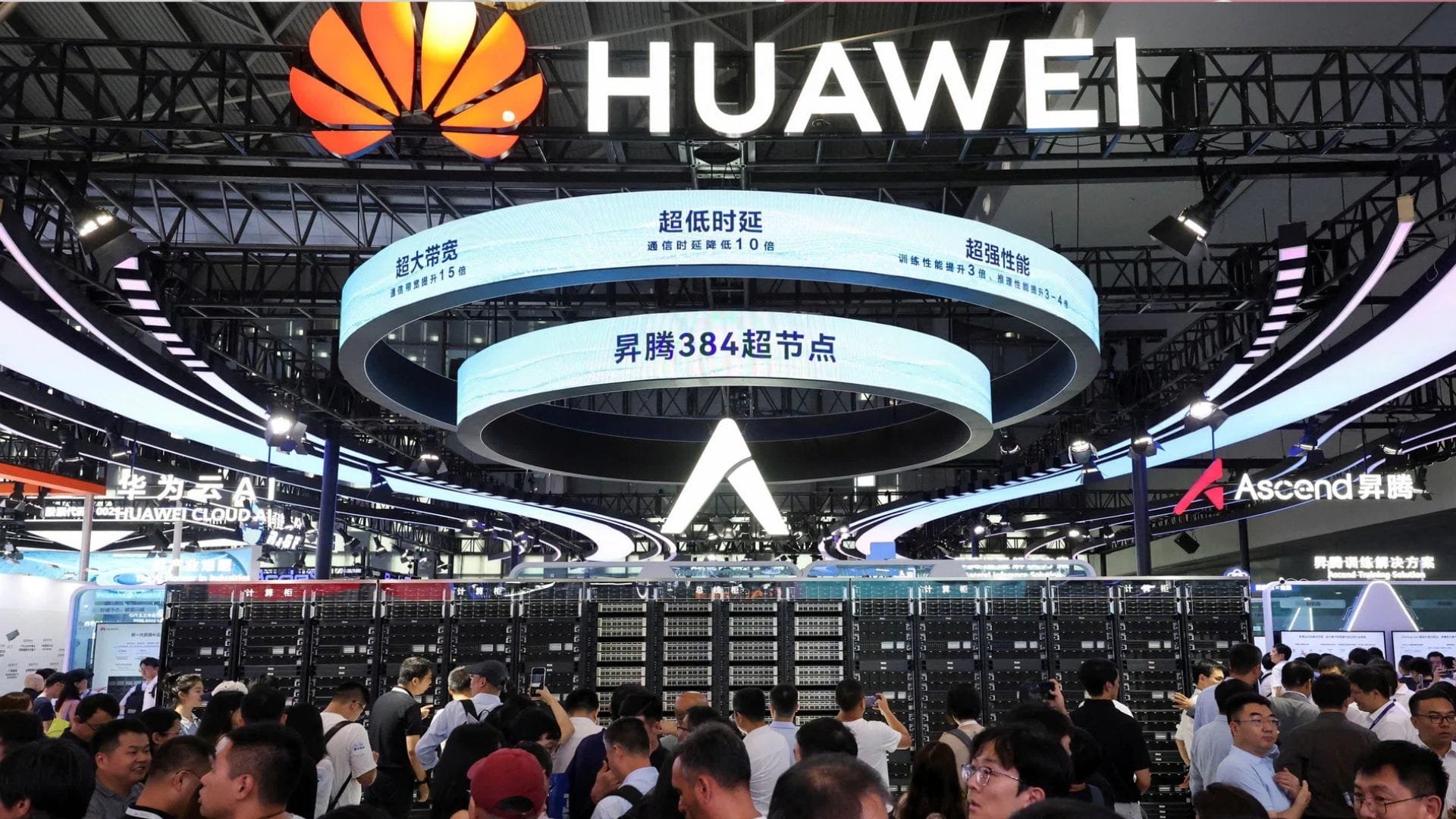
Huawei has announced a new chip design strategy that it believes could help the company overcome the impact of long-running US sanctions and develop processors with performance levels comparable to future 1.4nm-class chips.
The Chinese technology company revealed the approach nearly six years after losing access to advanced overseas semiconductor manufacturing partners. Since restrictions were introduced, Huawei has faced major challenges in producing cutting-edge chips for smartphones, artificial intelligence systems and data centres.
Rather than depending entirely on smaller manufacturing processes, Huawei said its new approach focuses on improving how information moves within chips and computing systems. The company described the strategy as a shift away from the traditional race towards increasingly smaller transistor sizes.
Taiwan Semiconductor Manufacturing Company, better known as TSMC, only recently started mass production of 2nm chips and is expected to move towards 1.4nm manufacturing around 2028. Huawei’s announcement suggests the company is seeking alternative methods to narrow the technological gap, despite limited access to advanced foreign manufacturing technologies.
Huawei shifts focus from manufacturing nodes to chip architecture
Huawei has named its new design philosophy the “Tau Scaling Law”. According to the company, the strategy aims to improve chip efficiency by reducing the time needed for signals and data to travel through processors and connected computing systems.
The company said the initiative is built on a new architecture called “LogicFolding”. Huawei explained that the architecture reduces internal wiring inside chips and shortens communication paths between components, potentially improving performance and energy efficiency.
Huawei stated that its Kirin mobile processors will be the first products to adopt the Tau Scaling architecture. The company believes the new design could deliver major performance improvements, even if manufacturing processes remain behind those of leading global chipmakers.
The announcement reflects a broader trend within the semiconductor industry, where companies are increasingly exploring alternative methods to improve computing power. While smaller transistor sizes have traditionally driven chip performance gains, rising production costs and technical complexity have pushed firms to investigate new architectural designs and packaging technologies.
Huawei’s strategy also highlights the pressure Chinese technology firms face following restrictions on access to advanced semiconductor equipment and manufacturing services. Since the sanctions were introduced, Chinese companies have been forced to invest heavily in domestic research and alternative chip development methods.
Ascend AI chips expected to adopt LogicFolding by 2030
Huawei also confirmed that its Ascend artificial intelligence chips are expected to adopt the LogicFolding architecture by 2030. The company’s AI processors have become increasingly important in China’s growing artificial intelligence and cloud computing sectors.
The Ascend series is already used in data centres and AI training systems across China. By introducing the new architecture into these products, Huawei hopes to improve processing performance while addressing some of the limitations associated with current manufacturing restrictions.
The company suggested that the Tau Scaling strategy could eventually support more advanced AI workloads and help Chinese firms compete more effectively in global computing markets. The move comes as demand for AI chips continues to increase worldwide, driven by the expansion of generative AI tools and large-scale computing models.
Industry observers have noted that Huawei’s latest announcement demonstrates China’s determination to strengthen its domestic semiconductor capabilities. With access to some foreign technologies restricted, Chinese firms are increasingly investing in home-grown alternatives across chip design, manufacturing and software development.
Huawei’s plans could also influence how other Chinese semiconductor companies approach future development. Instead of competing solely on manufacturing node sizes, companies may focus more heavily on architectural innovations designed to maximise performance using existing production technologies.
Technical challenges remain despite the ambitious roadmap
Despite presenting an ambitious vision, Huawei acknowledged that significant technical obstacles remain before the Tau Scaling approach can be widely implemented.
One of the main challenges involves developing entirely new chip design tools capable of supporting the new architecture. Existing semiconductor design software has largely been built around conventional scaling methods, meaning Huawei may need to create customised tools for its future processors.
The company also highlighted concerns surrounding heat management and thermal efficiency. Denser, more complex chip layouts can lead to overheating, particularly in high-performance processors used for artificial intelligence and data centre operations.
Analysts believe overcoming these engineering difficulties will require years of research and substantial investment. However, Huawei’s announcement suggests the company is committed to pursuing long-term semiconductor independence despite continuing geopolitical and technological pressures.
If the strategy succeeds, it could have implications beyond Huawei itself. The development may support China’s broader efforts to build a more self-sufficient semiconductor ecosystem, even as access to advanced international manufacturing technologies remains heavily restricted.
Huawei’s latest roadmap also signals a possible shift in how the global semiconductor industry measures progress. While manufacturing node sizes have long been viewed as the primary benchmark for chip advancement, companies may increasingly explore alternative architectures and system-level efficiency improvements to deliver future performance gains.